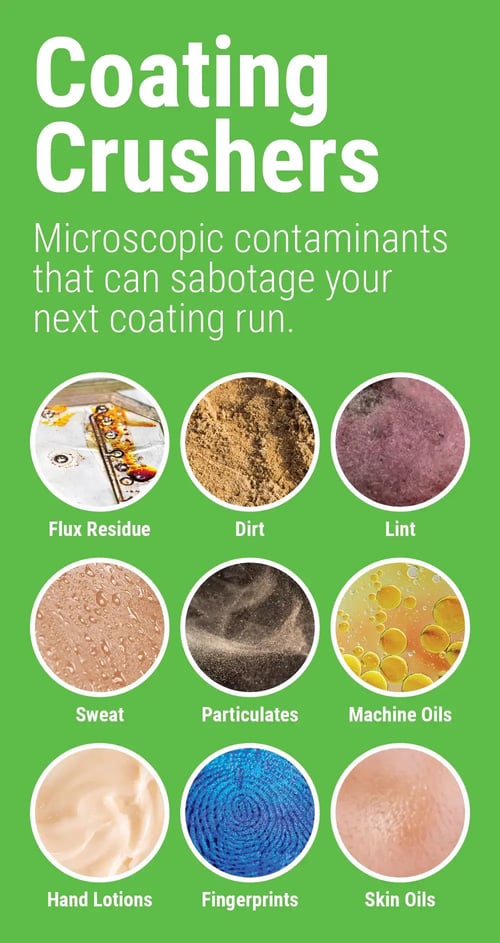


Overview & Key Takeaways
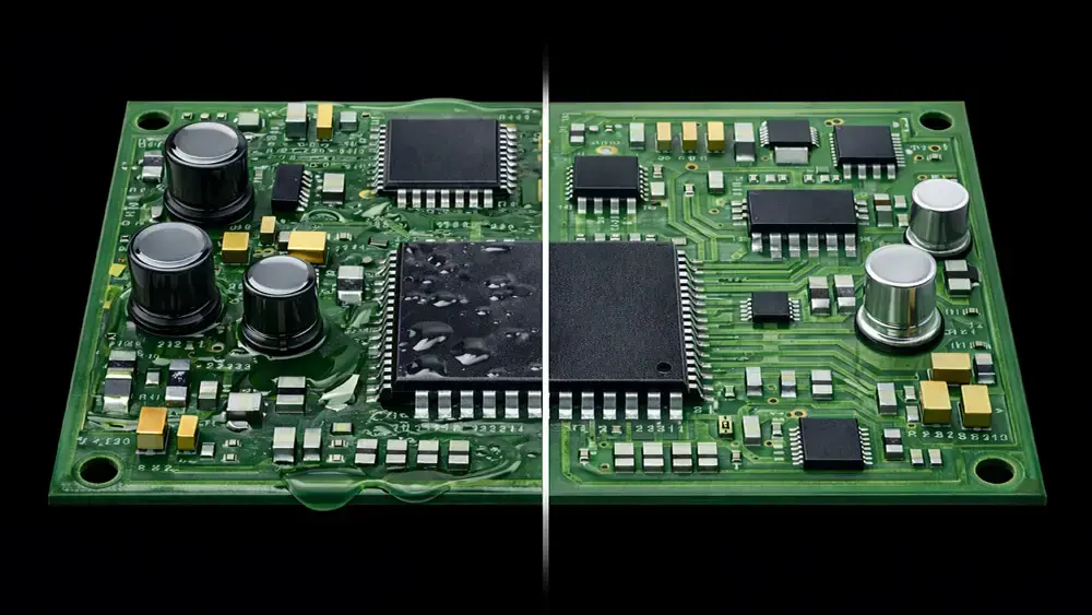
This guide provides engineers with a practical, side-by-side comparison of Parylene coatings vs. traditional liquid conformal coatings to support informed material selection for high-reliability electronics. While both technologies offer protection against moisture, corrosion, and electrical failure, their performance, application methods, and long-term reliability differ significantly.- Parylene provides highly uniform coverage: Its vapor deposition process creates a thin, pinhole-free coating that evenly protects complex geometries, including edges, gaps, and under components.
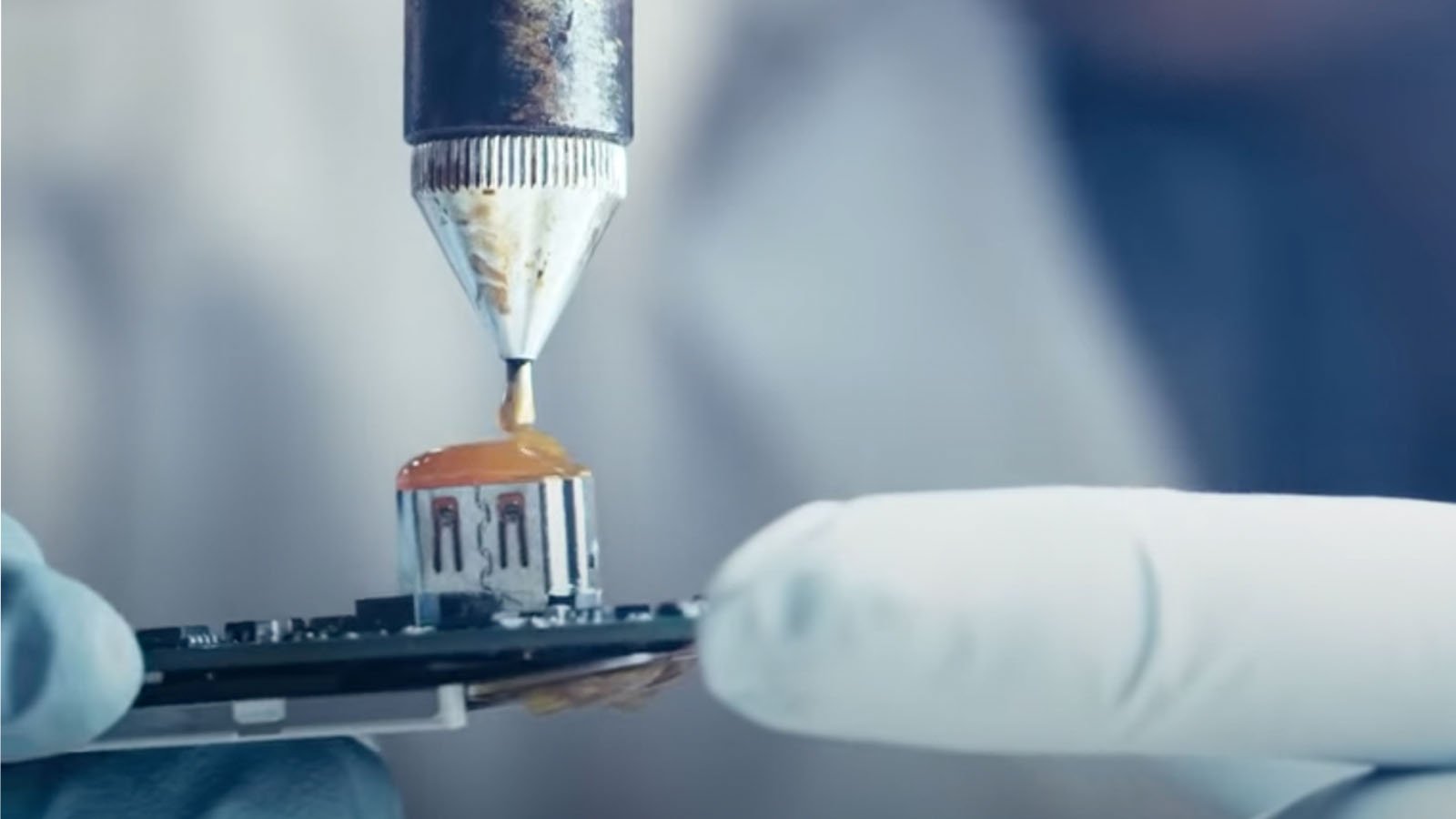
- Liquid coatings are more variable in application: Spray, dip, or brush methods can lead to uneven thickness, including pooling, edge thinning, and shadowing around dense components.
- Parylene offers superior barrier protection: It delivers strong resistance to moisture, chemicals, and environmental exposure, making it well-suited for harsh and high-reliability applications.
- Electrical performance is more consistent with Parylene: High dielectric strength and low dielectric constant support compact designs and reliable insulation performance.
- Thinner coatings can achieve high performance: Parylene typically meets protection requirements at much lower thicknesses compared to liquid coatings.
- Liquid coatings can be more cost-effective for simpler use cases: They are often easier to apply at scale and may be sufficient for less demanding environments.
- Both technologies can meet industry standards: However, Parylene generally provides greater consistency and reliability across a wider range of operating conditions.
- Material selection should be application-driven: Parylene is ideal for mission-critical, miniaturized, or harsh environments, while liquid coatings are often chosen for cost-sensitive or lower-risk applications.
Key performance differences between Parylene and liquid films
Engineers evaluating environmental protection for their electronics often hear two broad options: traditional liquid conformal coatings (acrylic, urethane, silicone, epoxy) and vapor-deposited Parylene. On paper, both categories promise corrosion resistance, dielectric insulation, and improved reliability – but their performance envelopes and trade-offs differ.
Material Properties
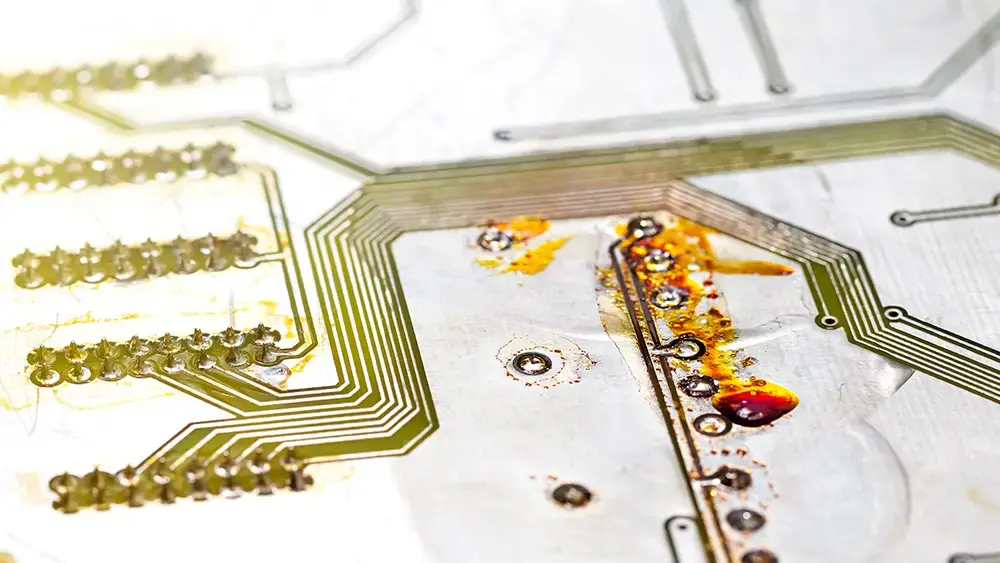
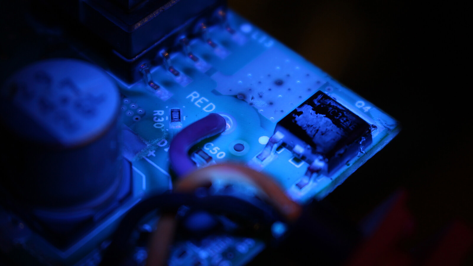
A structured comparison starts with material properties. Parylene films, deposited via chemical vapor deposition (CVD), form ultra-uniform, pinhole-free layers that completely encapsulate complex three-dimensional geometries. Because they are deposited in a vacuum directly from the gas phase, they exhibit extremely low water vapor transmission, high dielectric strength, and excellent chemical inertness at thicknesses often half of what a liquid conformal coating would require to meet the same standard. Liquid conformal coatings, by contrast, are applied from solution. Issues like edge-thinning, pooling, and coverage shadows must be actively managed, especially around sharp leads, tall components, and under low-standoff packages. These coatings can still perform well in many environments, but they generally need to be thicker to compensate for coverage variation. Their permeability and long-term stability in the presence of aggressive fluids are typically inferior to Parylene.
Electrical Performance
Electrical performance is another key differentiator. Parylene’s combination of high dielectric strength and low dielectric constant supports tight creepage and clearance distances, high-speed signaling, and compact high-voltage designs. Liquid coatings vary widely by chemistry, and some, such as silicones, can deliver good electrical insulation, but they do not match Parylene’s combination of thinness and robustness. When comparing performance, it is important to anchor the discussion in recognized standards and test methods. Documents such as IPC-CC-830 and IPC-HDBK-830 define qualification tests – dielectric withstand, insulation resistance, thermal shock, and more – that any coating technology must pass. External resources, such as this technical overview of IPC-CC-830, provide helpful background for teams new to these standards. In practice, both Parylene and liquid coatings can be engineered to pass such tests. The distinction emerges over the product lifecycle: how coatings behave after years of thermal cycling, exposure to mixed contaminants, and mechanical stress. Here, the consistency and barrier strength of Parylene give it a clear edge for mission-critical applications, while liquids may be entirely adequate for less demanding environments.
Process, throughput, and cost tradeoffs engineers must weigh
Once engineers understand the performance deltas, the next question is practical: how do process, throughput, and cost compare – and where do they tip the decision one way or the other? Liquid coatings are typically applied by spray, dip, or selective coating equipment. They can be integrated directly into SMT or box-build lines, and with the right fixturing and robotics, they support high throughput. Drying and curing steps add time and WIP, but continuous ovens and UV curing can compress that overhead. Material cost per unit area is relatively low, although multi-pass spray processes can increase consumption.
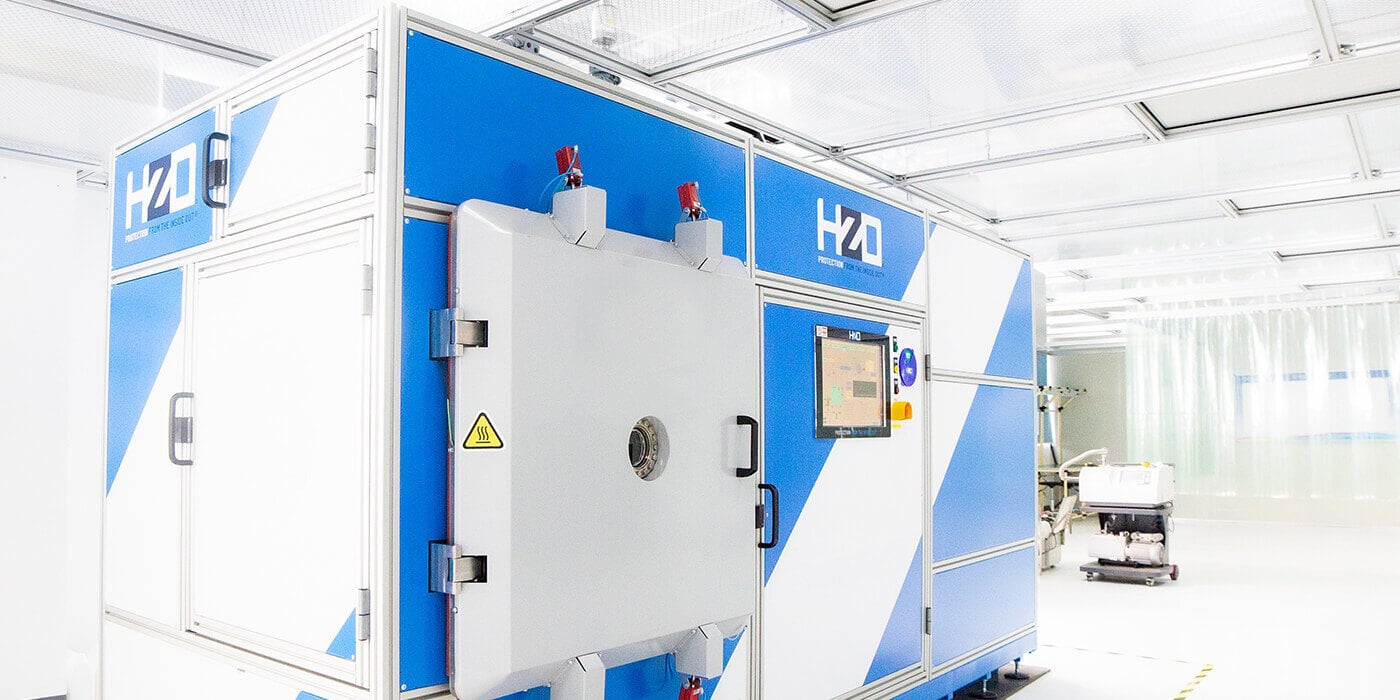
Parylene, by contrast, is a batch vacuum process. Assemblies are loaded into a chamber, masked areas protected, and a defined amount of dimer is vaporized and polymerized until the target thickness is reached. There is no liquid phase, so there is no drying or curing, and no VOCs to manage. Cycle times are measured in hours, and throughput is managed by optimizing chamber loading and recipe time. For low to medium volumes, especially in medical or industrial markets, this batch nature is often acceptable. In high-volume segments such as consumer electronics and automotive, the key is industrialization: well-designed racks that maximize chamber density, robust masking strategies, and process controls that minimize variation. Resources like HZO’s conformal coating guide and its thin-film webinar series can help internal teams understand these dynamics.
Cost
Cost needs to be considered at a lifecycle level, not just per-unit process cost. Liquid coatings look inexpensive from a BOM and line-time standpoint, but field failures, returns, and latent corrosion can easily erase that advantage. Parylene’s per-unit processing cost is higher, but its barrier performance, electrical insulation, and long-term stability often translate into fewer failures and warranty claims. From a supply-chain perspective, Parylene also opens up design options that can reduce system-level cost. For example, replacing bulky mechanical seals with a thin-film barrier can enable smaller housings, lower material usage, or simplified assembly steps. In some applications, it may allow the use of lower-cost substrate materials because the coating provides the needed environmental robustness. The key for decision-makers is to model both direct and indirect costs. Look beyond cycle time and dimer price to include the cost of field returns, rework, safety margins in design, and even reputational impact. Many organizations find that for a subset of mission-critical assemblies, Parylene is the more economical choice once the full picture is visible.
When to specify Parylene and when liquids are sufficient
Ultimately, the decision to use Parylene or a liquid conformal coating should be made at the design stage, informed by reliability targets, regulatory requirements, and business constraints. As a starting heuristic, Parylene tends to be the right fit when:
-
The assembly operates in a harsh or mixed environment (liquids, salts, industrial gases, biological fluids)
-
Failure carries high safety, regulatory, or brand risk
-
Dense circuitry and fine pitch increase the risk of leakage and arcing
-
There is value in shrinking the form factor or simplifying mechanical sealing
-
Qualification to demanding standards such as IPC-CC-830, UL 746E, or medical biocompatibility is required
Liquid coatings remain a strong choice when:
-
The environment is moderate and mostly limited to humidity or occasional condensation
-
Assemblies are easily accessible for rework and replacement
-
Time-to-market and line simplicity outweigh maximum robustness
-
Coating is used primarily as a cleanliness and dust barrier rather than a primary corrosion or chemical barrier
In many organizations, the most effective strategy is a hybrid one: reserve Parylene for the 10–30% of products where its capabilities align with high criticality and severe environments, and use optimized liquid coatings elsewhere. This portfolio view aligns coating spend with risk while leveraging existing infrastructure. Engineers and program managers can strengthen their case for the right coating choice by referencing external technical resources.
Overviews of conformal coating standards, such as IPC-CC-830, and design handbooks, like IPC-HDBK-830, can provide a neutral framework for internal discussions. By combining those references with HZO’s own data on Parylene performance – for example, its work on high-dielectric-strength, low-permeability films and scalable deposition chambers – engineering teams can build a clear, evidence-based story: where Parylene is essential, where liquids are sufficient, and how to implement both efficiently. With this clarity, coating stops being a late-stage checkbox and becomes an integral part of how reliable, high-performing products are engineered from day one.